Precision-engineered hardware platforms configured for fabless labs, high-throughput OSAT testing, and wafer parametric inspection.
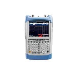
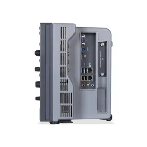
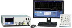
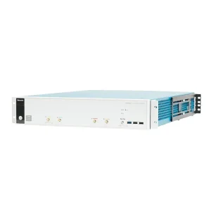
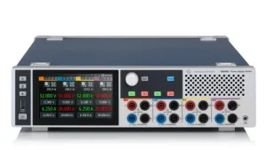
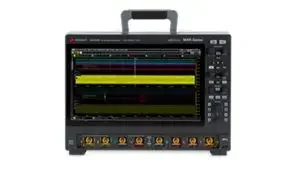
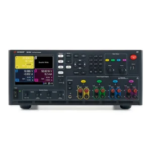
As lithography transitions below 3nm and packaging shifts toward 2.5D/3D chiplet heterogeneous architectures, the cost of silicon failure escalates exponentially. Test engineering departments require agile wholesale channels to secure verified, high-performance measurement instruments with zero lead-time compromises.
Design validation engineers face unprecedented challenges with gigascale SoCs. Demands center on sub-femtosecond jitter characterization, multichannel digital stimulus generation, and precision dynamic current profiling down to picoamperes to guarantee power envelope integrity during deep-sleep and high-compute transitions.
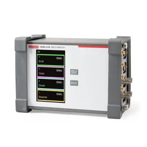
Wafer-level reliability (WLR) and inline parametric die testing require extreme throughput and sustained instrument up-time. Foundry test benches integrate automated source measure units (SMUs), ultra-fast C-V switches, and low-leakage matrix cards to map gate dielectric breakdown (TDDB) and hot-carrier degradation across 300mm wafers.
Outsourced Semiconductor Assembly and Test (OSAT) facilities are the primary consumers of wholesale automated test equipment (ATE). The explosion of multi-die CoWoS, FO-WLP, and 3D stacked dies demands Known Good Die (KGD) verification before bonding to avert costly package yield collapse.
Testing requirements diverge sharply across applications. We supply integrated test setups tailored to specific physical constraints, thermal extremes, and communication standards.
High-voltage powertrain electrification requires testing devices beyond 3kV and dynamic switching transients exceeding 100V/ns. Our solutions incorporate high-voltage curve tracers, sub-nanosecond optical isolation probes, and automated thermal chuck parametric analyzers to validate RDS(on) without destructive oscillation.
Mission-critical automotive silicon mandates strict zero-defect quality thresholds across -40°C to +150°C operating environments. Sourced test platforms streamline tri-temperature burn-in, electrostatic discharge (ESD) simulation, and high-temperature operating life (HTOL) continuous data-logging.
High-Performance Compute silicon demands unprecedented data bandwidth. Wholesale solutions cover 112G/224G PAM4 Bit Error Ratio Testers (BERT), multichannel sampling scopes, and PCIe Gen 5/6/7 protocol exercisers to rigorously inspect transmitter equalization, pre-shoot, and de-emphasis margins.
Next-gen wireless transceivers demand wideband vector signal analysis reaching sub-THz frequencies. We deliver modular instrumentation with phase noise floors surpassing -130 dBc/Hz at 10 kHz offset, enabling flawless EVM characterization across active antenna arrays and phased-array radar modules.
Navigating the trajectory of semiconductor validation from conventional planar silicon to sub-2nm Gate-All-Around (GAA) nodes and Co-Packaged Optics (CPO).
Die-to-die (D2D) interconnects introduce thousands of high-density micro-bumps requiring gigabit-per-second boundary scan without physical probe pin contamination. Test systems rely on advanced loopback built-in self-test (BIST) telemetry cross-correlated with multi-port high-frequency time-domain reflectometry (TDR).
As copper traces encounter severe reach limitations at 224 Gbps, optical transceivers integrate directly with compute silicon. Co-packaged optical testing demands combined electro-optical parameter analyzers capable of tracking polarization-dependent loss, relative intensity noise (RIN), and eye-diagram EVM in synchronized sweeps.
Modern ATE platforms interface directly with fab MES systems. Leveraging generative machine learning algorithms, modern test setups identify parametric drift patterns before structural defects materialize, drastically shrinking burn-in testing overhead while boosting overall final-test yields.
| Test Domain | Critical Measurement Parameters | Target Architecture | Primary Hardware Instrument Type | Yield Impact Factor |
|---|---|---|---|---|
| Wafer Parametric (WLR) | Vth, Ileak, Breakdown, C-V Curves | FinFET, GAAFET, Nanoribbon | High-Precision Multi-Channel SMU Rack | Prevents wafer fab misprocessing |
| Power Semiconductor | Dynamic RDS(on), Qrr, UIS, V(BR)DSS | SiC MOSFET, GaN HEMT, IGBT | Current Waveform Analyzers & Curve Tracers | Eliminates field catastrophic breakdown |
| High-Speed Digital | Eye Height/Width, TJ/DJ/RJ, SNDR, BER | PCIe 6.0/7.0, PAM4, CXL 3.0 | ATI High-Bandwidth Scopes & High-Rate BERTs | Guarantees interconnect interoperability |
| RF & Microwave | S-Parameters, Noise Figure, IM3, ACLR | 5G mmWave Front-Ends, SATCOM | Vector Signal Analyzers & Microwave VNAs | Secures spectral compliance & EVM |
| Dynamic Power Profiling | Current spikes (nA to A), Inrush, Rail Droop | IoT, Mobile SoC, Edge AI Cores | DC Power Analyzers with Fast ADC Logging | Maximizes battery cycle longevity |
Semiconductor fabrication facilities operate under tight capital depreciation deadlines. Equipment lead times extending past 52 weeks can delay multi-billion-dollar wafer fab production schedules.
Geopolitical fragmentation and export restrictions require tier-one semiconductor facilities to eliminate single-source hardware dependencies. Wholesale partnerships provide secondary validation lines with fully cross-compatible test scripts across major instrument ecosystems (Keysight, Rohde & Schwarz, Tektronix, Keithley).
Test economics represent up to 25% of total silicon manufacturing costs in complex mixed-signal systems. We help high-volume facilities drive test-parallelism from x16 to x64 sites per handler, deploy high-speed modular AXIe/PXIe chassis, and cut capital cost-per-pin without conceding measurement repeatability.
When a critical spectrum analyzer or real-time digitizer fails on an active semiconductor qualification line, production costs spiral immediately. Maintaining multi-hub inventory hubs across Hong Kong, Shenzhen, and Nanchang allows same-day dispatch and rapid cross-border logistics to restore line operations.
Structured end-to-end quality control ensuring verified serial numbers, calibrated accuracies, and compliance for mission-critical cleanroom installations.
Deep review of model options, bandwidth keys, software licenses, channel counts, and environmental specs.
Direct verification of physical probe heads, calibration substrate kits, and rack-mount form factors.
NIST/ISO 17025 accredited calibration, noise-floor profiling, and factory parameter re-verification.
Anti-static ESD barrier vacuum wrapping, multi-axis shock monitoring, and heavy-duty flight casing.
Complete dual-use EAR/ITAR export documentation, customs brokerage, and life-cycle repair support.
Precision semiconductor instruments require strict adherence to international legal, technical, and metrology standards.
Every supplied semiconductor test unit undergoes strict evaluation adhering to ISO/IEC 17025 quality frameworks. Measurement certificates demonstrate unbroken chain of traceability to the National Institute of Standards and Technology (NIST) or equivalent national metrology institutes, guaranteeing legal defensibility for customer fab audits.
High-speed oscilloscopes with bandwidths over 60 GHz, advanced optical modulation analyzers, and wideband RF synthesizers are tightly regulated under the Wassenaar Arrangement, US EAR, and EU Dual-Use regulations. Our compliance desk manages export licensing, End-User Statements (EUS), and classification determinations.
To safeguard Class 100/ISO Class 5 semiconductor fab environments, all test units are ultrasonically cleaned and sealed in ESD-safe barrier bags before dispatch. Furthermore, our dedicated repair depots provide component-level board diagnostics, attenuator replacements, and firmware calibrations long past OEM end-of-life (EOL).
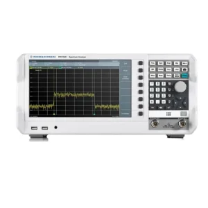
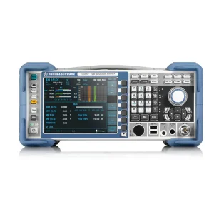
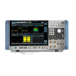
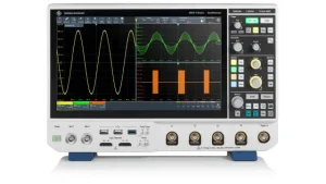
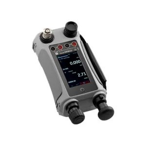
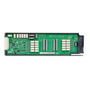
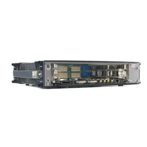
Expand your automated test footprint with top-tier spectrum analyzers, precision parameter analyzers, DAQ switching units, and pressure calibration standards.
Detailed technical and commercial answers addressing calibration validity, option keys, custom test integrations, and global logistics procedures.