Factory-certified calibration, signal characterization, and wideband diagnostic instruments engineered for high-density power source and adapter verification.
Bridging high-frequency power electronics with precision laboratory test standards to deliver uncompromised efficiency, thermal stability, and low-noise operational integrity.
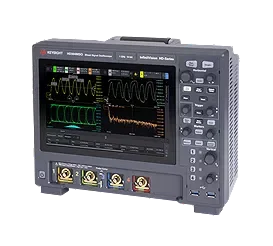
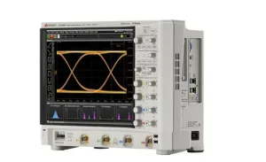
Modern power adapter architectures—ranging from gallium nitride (GaN) fast-charging modules to multi-kilowatt rack-mounted DC rectifiers—require sub-millivolt noise floor verification. Leveraging Keysight DSOS804A high-definition oscilloscopes and Tektronix IsoVu isolated current probes, engineers map parasitic inductive loops, ensuring absolute transient fidelity.
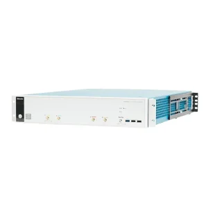
Silicon Carbide (SiC) and GaN FET topologies introduce ultra-fast dV/dt slew rates exceeding 100 V/ns. Validating high-speed switching transitions necessitates wideband oscilloscopes and real-time current waveform analyzers like CX3324A to prevent shoot-through currents, isolate ringing phenomena, and optimize gate driver impedance networks.
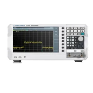
Electromagnetic compatibility (EMC) is fundamental to power converter reliability. Deploying Rohde & Schwarz R&S®FPC1000 spectrum analyzers with integrated quasi-peak detectors allows power adapter suppliers to isolate differential-mode and common-mode conducted emissions early in the prototyping phase, ensuring turnkey compliance with CISPR 32/EN 55032.
A deep technical analysis of semiconductor physics, magnetic component miniaturization, digital loop control, and bidirectional vehicle-to-everything (V2X) interfaces driving the power conversion sector.
Transitioning from legacy Superjunction MOSFETs to Wide Bandgap (WBG) materials eliminates reverse recovery charge (Qrr) and scales switching frequencies above 500 kHz. Utilizing Totem-Pole PFC combined with LLC resonant tank converters shrinks passive magnetic components by over 65%, driving power densities exceeding 35 W/in³.
ACF implementations recycle transformer leakage energy rather than dissipating it as thermal waste across passive RCD snubber circuits. Coupled with Zero Voltage Switching (ZVS), ACF topologies enable compact power adapters to operate cooler while exceeding EU CoC Tier 2 and US DoE Level VI statutory requirements.
The integration of high-speed ARM Cortex-M0+ and DSP-based microcontrollers into industrial power sources permits dynamic voltage scaling, cycle-by-cycle digital loop compensation, and standardized PMBus/I2C/CAN bus real-time reporting of thermal runaways, component health, and cumulative power hours.
Modern power conversion extends beyond unidirectional AC-DC rectification. Emerging dual-active bridge (DAB) and bi-directional buck-boost architectures transform high-power adapters into grid-tied energy nodes capable of vehicle-to-load (V2L) and microgrid balancing with reactive power compensation.
Turnkey power supply and custom adapter deployment frameworks engineered for demanding operating environments, harsh thermals, and zero-fail operational requirements.
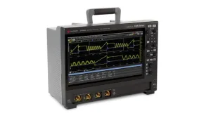
On-board chargers (OBC), DC-DC auxiliary power units, and external high-voltage programming supplies must withstand load dump transients (ISO 7637-2/ISO 16750-2). Our integrated testing infrastructure utilizes Tektronix MSO22/MSO24 and multi-channel DAQ systems to monitor thermal gradient stability under 800V silicon-carbide bus stresses.
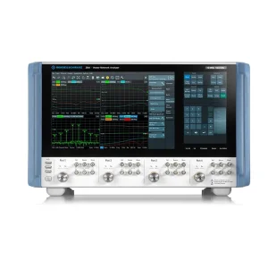
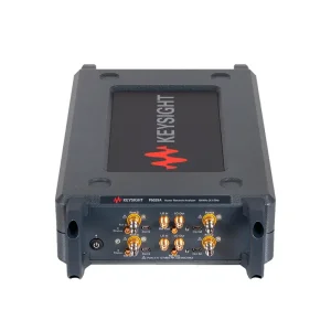
Hyperscale AI data centers demand CRPS (Common Redundant Power Supply) solutions with 96%+ 80 PLUS Titanium efficiency. Power adapters powering optical transceivers and remote edge radios are qualified using Keysight P5004A Vector Network Analyzers to eliminate microwave jitter and high-speed bus clock cross-talk.
Medical grade AC-DC power supplies require 2x MOPP (Means of Patient Protection), reinforced 4000 VAC isolation, and touch leakage currents strictly below 100 μA. In-line automated production fixtures verify dielectric breakdown resistance and transient recovery across medical diagnostic monitors and surgical tools.
Harnessing the Greater Bay Area’s hyper-dense industrial cluster: automated surface-mount manufacturing, localized silicon wafer foundries, and integrated quality verification architectures.
Smart assembly lines incorporate high-speed Yamaha and Fuji pick-and-place systems capable of mounting 01005 passives and ultra-fine pitch planar transformers. Automated Optical Inspection (AOI) coupled with 3D X-ray Inspection (AXI) confirms void-free solder joints under quad-flat no-leads (QFN) power control packages, eliminating hidden field failures.
The geographic proximity of core magnetic core manufacturers, custom ferrite extrusion plants, Class-H insulated copper wire producers, and specialized electrolyte capacitor vendors in Shenzhen and Dongguan compresses engineering turnaround. Prototype custom magnetic chokes are iterated in 48 hours rather than weeks.
Every manufactured power source undergoes computerized burn-in stress screening under full thermal load while linked to our Cloud Manufacturing Execution System (MES). Unique 2D datamatrix codes laser-etched onto PCB substrates trace the exact component wafer lot, SMT machine telemetry, and ATE test data.
Rigorous qualification protocols for international original equipment manufacturers: evaluating thermal derating curves, component obsolescence lifecycles, and risk-mitigated supply chains.
| Evaluation Dimension | Conventional Commercial Supplier | Tier-1 Industrial Metrology Standard | Strategic OEM Business Impact |
|---|---|---|---|
| Semiconductor Class | Standard Planar Silicon MOSFET | GaN / SiC High-Frequency | Reduces chassis thermal load by 40%, enables sub-compact form factors. |
| Ripple & Noise Density | < 100 mV Peak-to-Peak | < 20 mV Metrology-Grade | Eliminates analog sensing drift and high-speed communication bit errors. |
| Burn-in Protocol | Sample Batch Testing (2-4 hrs) | 100% 4-Corner ORT (12-24 hrs) | Guarantees zero early infant mortality at end-user installation sites. |
| Electrolytic Life (Caps) | 2,000 hrs @ 85°C Standard | 10,000 hrs @ 105°C Solid Polymer | Extends continuous system operating life beyond 7+ years without servicing. |
| Supply Continuity | Single-Foundry Exposure | Multi-Fab Pin-to-Pin Dual-Source | Safeguards continuous procurement lines against geopolitical and fab disruptions. |
Multinational regulatory clearance, field-application engineering (FAE) support networks, and ISO/IEC 17025 accredited laboratory test validations.
Harmonized safety standard covering hazard-based engineering across audiovisual, IT, and communication equipment.
Full compliance with Low Voltage Directive (LVD) 2014/35/EU, EMC Directive 2014/30/EU, and RoHS 2011/65/EU.
Precision radiated and conducted RF interference boundaries qualified inside 10-meter semi-anechoic test chambers.
Extreme no-load standby power dissipation restricted to < 75 mW, with ultra-high average active efficiency compliance.
Certified for multi-market customs import: PSE (Japan), KC (Korea), CCC (China), RCM (Australia), and BIS (India).
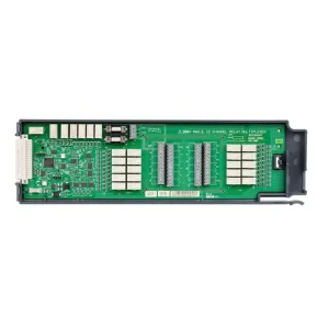
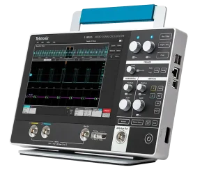
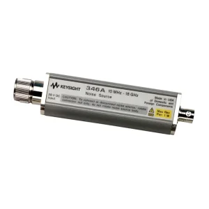
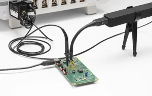
High-speed modular digitizers, current probes, and precision electrical calibrators required for production line qualification and validation.
Direct answers from our senior power electronics engineers and supply chain directors addressing qualification standards, topology selection, and customs documentation.
Gallium Nitride (GaN) features a bandgap of 3.4 eV compared to Silicon's 1.1 eV, yielding a breakdown electric field ten times greater and switching speeds an order of magnitude faster. Because GaN switches exhibit minimal gate charge and virtually zero reverse recovery charge, engineers can transition from 65 kHz to upwards of 300 kHz–1 MHz. This reduces the volumetric space required for magnetics (transformers and inductors) and heat-sinks, yielding 95%+ efficiency in half the physical envelope.
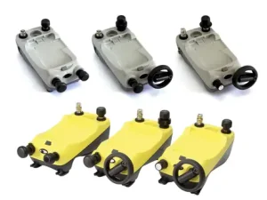
We operate a multi-tier anti-counterfeiting verification regime. Every semiconductor, passives lot, and turnkey instrument sourced from manufacturers such as Keysight, Rohde & Schwarz, Tektronix, and Druck undergoes incoming goods verification. We audit laser lot codes, inspect lead integrity with digital microscopy, compare against OEM silicon datasheets, and cross-reference unique serialized certificates of conformance before integration or export dispatch.
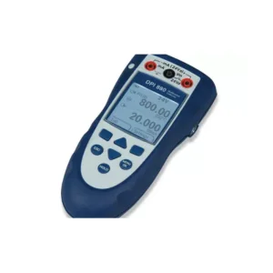
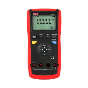
All high-accuracy power sources and measuring devices can be delivered with a fully accredited ISO/IEC 17025 certificate of calibration. The calibration process checks zero-drift, linearity across current shunts, harmonic content analysis, and full-scale voltage precision referenced to national metrology standards (NIST / NIM). Reports include ambient environmental records, measurement uncertainty figures, and calibration due intervals.
Our strategic supply architecture maintains dual-track inventory buffers in Hong Kong and Shenzhen free-trade hubs. By partnering directly with over 2,000 qualified raw-material fabricators and maintaining second-source pin-to-pin functional equivalents for active semiconductors and magnetic cores, we insulate clients from single-foundry allocation halts, keeping OEM deliveries within verified 4-to-6 week procurement windows.
Yes. We specialize in custom OEM/ODM power solutions ranging from open-frame board-level converters to IP67 ruggedized external power bricks. Our engineering teams assist with custom transformer winding design, thermal molding simulation, EMI PCB layout optimization, firmware development for PMBus telemetry, and mechanical enclosure injection tooling tailored to your system constraints.
All outbound shipments are packed according to international air and ocean cargo standards for delicate metrology and electronic loads. This includes anti-static vacuum-sealed barrier pouches, custom-molded closed-cell EPE shock-absorbent foam inserts, multi-wall corrugated external cartons, and integrated Drop-N-Tell / Tip-N-Tell vibration-sensing impact indicators to ensure pristine condition upon arrival across 100+ global destinations.