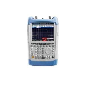
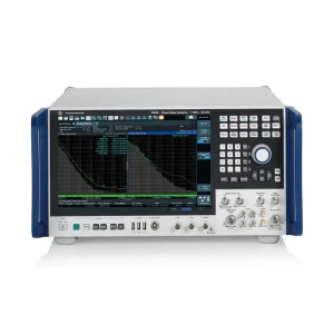
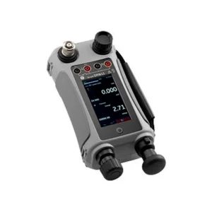
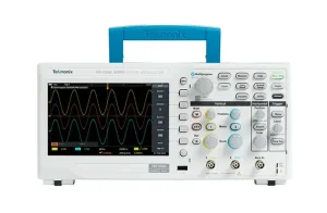
Direct supply and systems integration of calibrated high-speed oscilloscopes, logic analyzers, RF analyzers, and field calibration standards sourced directly from world-class OEMs.
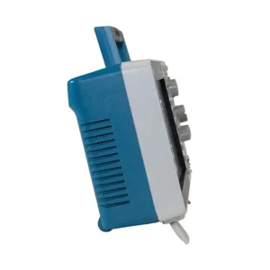
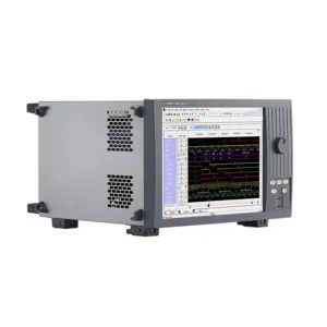
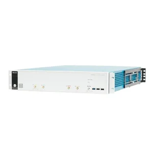
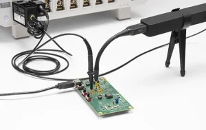
Strategic analysis of surface mount technology (SMT) verification, structural defect coverage, and high-throughput production paradigms across tier-1 manufacturing hubs.
Global EMS facilities in North America, Europe, and Southeast Asia are moving beyond pure unpowered analog ICT. The industry standard mandates hybrid architectures integrating analog unpowered guarding, powered analog/digital vector engines, and non-intrusive boundary-scan (IEEE 1149.1 / 1149.6).
With high-density interconnect (HDI) designs, test pads have contracted below 0.35 mm (14 mil), challenging spring probe mechanical targeting and test pad fatigue limits. Turnkey systems require FEA-modeled probe displacement to prevent board flexure during vacuum or pneumatic actuation.
International procurement requires a predictable supply chain capable of handling multi-vendor hardware ecosystems. From Keysight 3070 and Teradyne platforms to customized benchtop instrumentation, certified exporters bridge the gap between OEM backlogs and tight project deadlines.
A granular look at the critical electrical and mechanical building blocks that deliver zero false-call rates, precision component guarding, and maximum test coverage.
The core limitation in passive component testing within an assembled network is the presence of parallel circuit paths. Custom in-circuit test architectures utilize precision op-amp guarding techniques (virtual ground nodes) to cancel shunt currents. When evaluating resistor R1 in parallel with R2 and R3, an operational amplifier enforces identical potential across R2, driving the shunt current to zero and isolating R1 with laboratory-grade uncertainty.
Furthermore, our exporter integration incorporates 6-wire Kelvin bridges for sub-ohm contact resistance elimination, indispensable when validating automotive current-sensing shunts or low-loss inductors in modern power conversion stages.
Routing signals from high-pin-count PCBAs to the central measurement unit requires a reconfigurable, low-noise relay switching matrix. Systems supplied by Machine-Win feature reed-relay switching cards designed for ultralow thermal EMF (< 1µV) and parasitic capacitance under 15 pF per channel.
Whether configuring a 1:1 dedicated pin-to-node topology for high-volume consumer lines or a flexible multiplexed matrix architecture (e.g., 8-to-1 or 16-to-1 multiplexing) for high-mix low-volume aerospace assemblies, the system ensures negligible insertion loss and cross-talk suppression up to 50 MHz.
The mechanical fixture interface converts board Gerber data into physical spring-probe contact. Our export-ready custom solutions offer three standard fixture mechanisms:
Where physical probe access is restricted due to BGA ball arrays or high routing density, integrated IEEE 1149.1 / 1149.6 boundary-scan controllers take over. By driving scan chains through the device under test (DUT), systems verify pin continuity, solder opens, and bus integrity across digital transceivers without test pads.
In addition, vectorless test technologies (such as TestJet, capacitive diode sensing, or inductive sensing) detect open pins on IC connectors and discrete IC leads without needing test vector generation programs.
| Evaluation Parameter | Bed-of-Nails ICT | Flying Probe Test (FPT) | Boundary Scan (JTAG) | Functional Test (FCT) |
|---|---|---|---|---|
| Test Speed / Throughput | Extremely Fast (10 - 25s per board) | Slow (3 - 15 minutes per board) | Fast (5 - 20s per chain) | Medium to Slow (1 - 5 mins) |
| Defect Localization | Pin-point to discrete component/lead | Pin-point to discrete component/lead | Net-level and boundary-pin level | Subsystem or module level |
| Fixturing Cost & NRE | High NRE ($2,000 - $12,000) | Zero NRE (Software programmed) | Very Low (Software design) | High Custom NRE |
| Physical Access Dependency | High (requires test points/pads) | High (probes pads and traces) | Low (requires TDI, TDO, TCK, TMS) | Low (I/O connectors only) |
| Best Production Stage | High-Volume Mass Manufacturing | NPI, Prototypes & High-Mix Low-Volume | Dense Digital Boards, BGA verification | Final End-of-Line Quality Gate |
Targeted in-circuit test architectures customized for automotive electrification, aerospace avionics, medical implants, and high-frequency communication servers.
Zero-defect compliance under ISO 26262 ASIL-D. Specialized in battery management systems (BMS), 800V silicon carbide (SiC) traction inverters, and high-voltage DC-DC converters.
Ensuring compliance with DO-254 and MIL-STD-883 standards. Validating avionics flight control computers, phased-array radar sub-modules, and telemetry electronics.
Stringent compliance with ISO 13485 and FDA 21 CFR Part 11 requirements. Systems custom-engineered for patient monitors, surgical robotics, and implantable telemetry.
Addressing extreme heat and signal density in AI accelerator cards, PCIe Gen5/6 accelerator boards, and millimeter-wave active antenna units (AAUs).
Ensuring frictionless international deployment with comprehensive regulatory compliance, serial traceability, and precision packaging.
Every in-circuit test module, digitizer, multimeter unit, and signal analyzer distributed by Machine-Win undergoes strict quality control. All items are delivered with verifiable factory serial records, authentic documentation, and calibration traceable to national standards (NIST / CNAS / DKD) under ISO/IEC 17025.
Test equipment and bed-of-nails fixtures contain delicate mechanical tolerances and high-sensitivity optical/pneumatic assemblies. We utilize custom moisture-barrier hermetic sealing, desiccants, heavy-duty anti-static barrier bags, and spring-isolated floating base flight crates.
Operating strategic distribution centers in Hong Kong, Shenzhen, and Nanchang, Machine-Win delivers responsive engineering support across more than 100 countries. Our applications engineering teams support international buyers with fixture design consultations, test vector migration, and line-down rapid part dispatch.
Strategic technology developments reshaping PCBA structural testing over the next decade as semiconductor architectures shift toward multi-chip packaging.
Traditional ICT requires extensive manual trial-and-error to fine-tune guard ratios and eliminate parallel measurement errors. Next-generation systems incorporate machine-learning algorithms that analyze board netlists and real-time impedance matrices to dynamically synthesize the optimal multi-node guard matrix without human intervention, slashing fixture programming cycles by up to 70%.
With silicon advancement driving the rise of multi-die heterogeneous integration (2.5D/3D chiplets), testing boundaries are blurring between wafer-sort, bare-die probe, and PCB assembly. Modern ICT controllers are evolving to support high-speed serial test busses such as UCIe (Universal Chiplet Interconnect Express) alongside boundary scan for immediate die-to-die connectivity verification.
Real-time ICT parametric data is feeding directly back into solder paste printers (SPI) and pick-and-place systems. By capturing analog drift across thousands of test runs, predictive maintenance engines detect nozzle clogging, paste viscosity changes, and reflow profile shifts before a catastrophic assembly failure occurs on the manufacturing line.
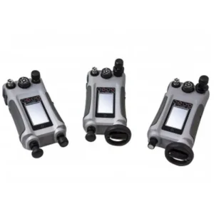
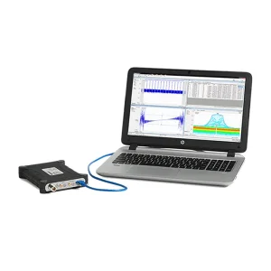
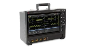
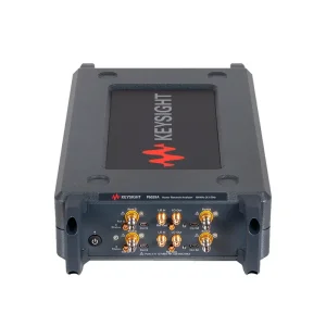
Original, brand-new equipment line-up including vector network analyzers, high-definition oscilloscopes, precision source measure units, and calibration references.
Expert answers addressing test architecture specification, fixture strain limits, global shipping protocols, and multi-vendor supply consolidation.