
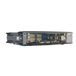
Direct sourcing and validated configurations for mission-critical laboratories, electronic testing racks, and automated semiconductor validation lines.
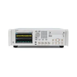
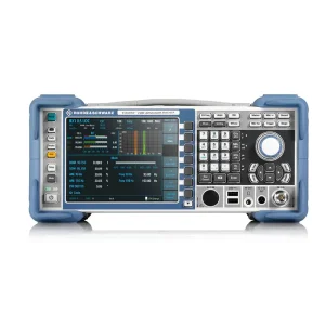
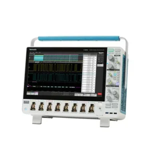
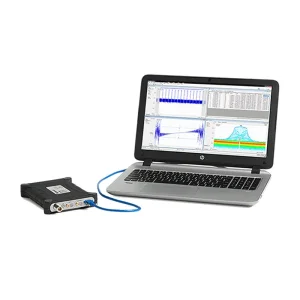
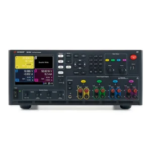
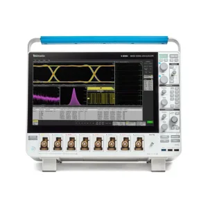
Bridging the gap between high-density AdvancedTCA (ATCA) telecom blades, micro-modular PXI Express solutions, and monolithic benchtop instruments.
The continuous exponential growth of serial interface velocities—transitioning through PCIe 5.0/6.0, 112Gbps/224Gbps PAM4, and coherent optical transceivers—has exposed substantial architectural limitations in traditional modular platforms. While standard PXIe excels in compact channel density, its standard 3U PCB surface area (approx. 160 cm²) and modest thermal dissipation headroom (typically 30W–58W per slot) impose severe constraints on complex DSP arrays, multi-core FPGAs, and high-frequency RF front-ends. AXIe (Advanced eXtension for Instrumentation and Test) directly resolves these thermodynamic and interconnect hurdles.
Inheriting the physical geometry and high-reliability foundation of the telecommunications industry standard AdvancedTCA (PICMG 3.0), AXIe establishes an expansive board surface exceeding 900 cm² per slot paired with power envelopes reaching up to 200W to 350W per slot. This allows precision test equipment manufacturers to integrate laboratory-grade signal generation, high-speed real-time sampling ADCs, and massive FPGA fabric onto a single hot-swappable blade while preserving picosecond-level synchronous triggering.
Over 5 times the usable PCB area of standard 3U PXIe. Accommodates multi-channel wideband ASICs, uncompromised ground shielding cans, and massive on-board DDR buffers without component stacking.
Dedicated point-to-point differential local bus, 100 MHz low-jitter reference clocking, and sub-nanosecond hardware trigger lines ensure deterministic multi-chassis channel synchronization.
Push-pull intelligent fan trays coupled with zoned aerodynamic air channels manage high-density 200W+ thermal loads effortlessly, maintaining device junction temperatures within calibrated tolerances.
To assist senior test architects and procurement directors in optimizing capital expenditure, the table below provides a rigorous technical comparison between prevalent instrumentation form factors:
| System Specification | AXIe Standard (1.0 / 2.0) | PXI Express (PXIe) | AdvancedTCA (ATCA) | Discrete Benchtop Systems |
|---|---|---|---|---|
| PCB Area per Slot | ~900 cm² (Horizontal / Vertical) | ~160 cm² (Compact 3U) | ~900 cm² (PICMG 3.0) | Enclosed dedicated chassis |
| Power Headroom per Slot | 200W – 350W | 30W – 58W (Chassis dependent) | Up to 300W | Self-contained internal PSU |
| Primary Data Fabric | PCIe Gen 3 / Gen 4 (x4, x8, x16) + LAN | PCIe Gen 2 / Gen 3 (x1, x4, x8) | 10G / 40G / 100G Ethernet | GPIB, USB-TMC, 10GbE LAN |
| Trigger Jitter / Skew | < 5 ps RMS (AXIe-1 timing spec) | < 25 ps RMS | Asynchronous (Telecom focus) | Cable-dependent BNC/SMA deskew |
| Target Deployment | High-speed BERT, AWG, 800G+ Optical, Semi ATE | Automated DAQ, Low-Power RF, Modular DMM | Telecom infrastructure, Cloud Switching | Manual benchtop R&D, standalone metrology |
| Rack Density Optimization | Maximum (Up to 14 slots in 4U/9U) | Moderate (Up to 18 slots in 4U) | High (Up to 14 slots in 12U/13U) | Low (Consumes substantial rack U space) |
Accelerating time-to-market for Tier-1 technology enterprises across demanding hyperscale telecommunications, semiconductor fabrication, and aerospace installations.
By housing high-order arbitrary waveform generators (such as 120 Gbaud AWG units) and multi-channel Bit Error Ratio Testers (BERT), AXIe provides the ultra-clean analog output and precise ISI jitter injection mandatory for validating next-gen QSFP-DD800 and OSFP optical modules.
Massive multi-pin digital test requirements demand sub-nanosecond pin-electronics deskew and high-speed vector memory. AXIe's dense backplane throughput allows parallel test sites to execute concurrently, lowering per-die test time and cutting device production costs dramatically.
Direct digital synthesis of wideband chirp waveforms and multi-emitter EW threat simulation requires microsecond-level pulse agility. Multi-channel AXIe digitizers sample coherent receiver arrays in phase-locked synchrony across multi-chassis test racks.
Autonomous vehicle processing stacks utilize multi-gigabit Automotive Ethernet (10GBASE-T1) and SerDes links. AXIe platforms execute compliance stress testing, packet error injection, and real-time physical layer eye diagram degradation analysis under harsh EMC conditions.
Multi-qubit gate manipulation demands ultra-low-noise DC biasing, microwave IQ mixing, and sub-10ns feedback loops. Modular AXIe FPGA blades deliver deterministic cryostat pulse generation without bulky interconnect bundles.
Characterizing wideband D-Band (110–170 GHz) and G-Band (140–220 GHz) signals requires processing intermediate bandwidths spanning over 30 GHz. AXIe's scalable modular digitizers deliver uncompressed streaming directly into high-throughput storage fabrics.
Pioneering optical backplanes, autonomous AI edge processing, and PCIe Gen 5/6 low-latency switching architectures.
As the international electronics sector embraces Compute Express Link (CXL) memory pooling, 224 Gbps PAM4 electrical signaling, and Co-Packaged Optics (CPO), the AXIe Consortium standards continue to advance rapidly. The upcoming iterations of high-density modular instrumentation are converging on four core pillars:
Next-generation backplanes implement PAM4 signaling at the copper trace level across the backplane backplane connectors, delivering aggregate bidirectional data throughput exceeding 128 GB/s per blade slot. This completely eliminates data transfer bottlenecks during multi-channel real-time acquisition.
Future AXIe blades are migrating to optical waveguide interconnects directly integrated into the chassis midplane. By bypassing legacy copper backplane traces, signal insertion loss is minimized, enabling near-zero latency clock distribution across wide chassis federations.
Instrumentation modules now integrate dedicated NPU / Tensor-processing silicon directly alongside ADCs/DACs. This architecture enables real-time autonomous eye-diagram masking, instant anomaly classification, and dynamic loop filter compensation before data leaves the blade.
Through active collaboration with precision calibration laboratories, high-density backplane connector specialists, and embedded Linux firmware consortia, our engineering network ensures that your infrastructure investments maintain a guaranteed backward-compatible migration path over a 10- to 15-year lifecycle.
Leveraging the world's most concentrated precision electronics ecosystem to compress delivery timelines, maintain critical component buffers, and optimize lifecycle costs.
In an era characterized by volatile global semiconductor allocations and extended lead times for specialized instrumentation, our strategic manufacturing and integration hub in the Shenzhen-Hong Kong Greater Bay Area (GBA) provides unprecedented procurement agility. Housing over 70% of the world's advanced electronics manufacturing infrastructure, this region empowers us to combine tier-1 brand instrument supply with bespoke modular enclosure fabrication and automated quality screening.
Our China Factory 4.0 integration facility utilizes end-to-end MES (Manufacturing Execution System) tracking. Every chassis, backplane, power supply module, and blade receives a unique cryptographic serial identifier. Prior to international containerization or courier dispatch, assemblies undergo rigorous burn-in thermal cycling, backplane eye-diagram margin testing, and vibration resonance screening to guarantee turn-on reliability immediately upon arrival at your overseas facility.
Mitigating cross-border operational risk with documented ISO/IEC 17025 metrology calibration, stringent export clearance, and measurable capital expenditure optimization.
By consolidating disparate single-function benchtop instruments into a unified AXIe chassis infrastructure, global labs slash floor space requirements, consolidate cooling overhead, and simplify central AC-to-DC power delivery.
Instruments and calibration references conform to international NIST/NIM traceable verification standards. Every high-speed digitizer, AWG, and power analyzer ships with comprehensive calibration certificates and baseline uncertainty reports.
Complete compliance with RoHS 3 (EU 2015/863), WEEE, CE, and FCC Part 15 regulations. Our logistics legal division handles customs classifications, HS tariff optimization, and Dual-Use export regulatory compliance seamlessly.
Expanding testing versatility across high-speed serial networks, RF spectrum analysis, multi-channel DAQ, and baseline metrology laboratories.
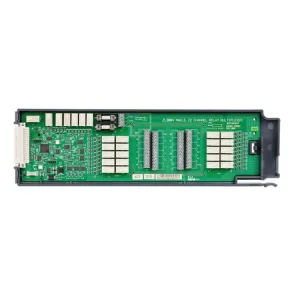
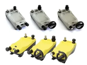
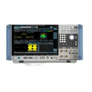
Detailed engineering answers addressing backplane bandwidth, driver compatibility, power distribution, and multi-vendor interoperability.