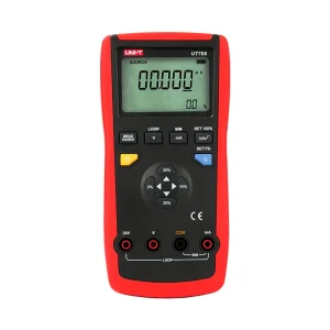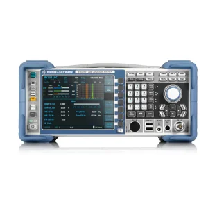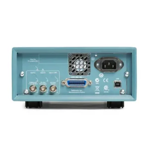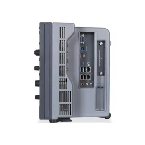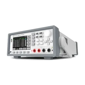
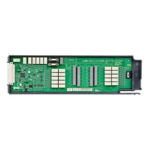
Engineered hardware and diagnostic platforms for validating dynamic load characteristics, switching efficiency, ripple noise, and electromagnetic compliance across custom power conversion nodes.
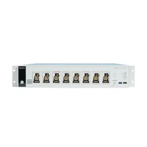
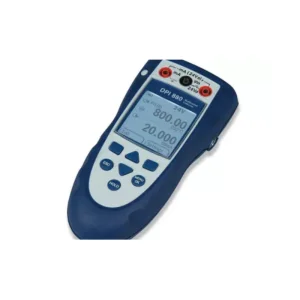
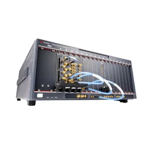
A rigorous breakdown of topology selection, magnetics design, and semiconductor gate drivers for custom AC-DC rectifiers and isolated/non-isolated DC-DC converters.
Standard switched-mode rectifiers utilize bridgeless totem-pole or interleaved boost PFC architectures to maintain power factor performance above 0.99 with total harmonic distortion (THD) under 3% across 85V-264V universal AC inputs.
For high-density DC-DC isolated conversion, LLC resonant topologies achieve zero voltage switching (ZVS) on the primary bridge and zero current switching (ZCS) on synchronous rectifiers, slashing frequency-dependent capacitive discharge losses.
Non-isolated intermediate bus converters (IBC) and point-of-load (PoL) regulators demand fast transient response with minimal output ripple. Multi-phase interleaved buck stages mitigate output capacitor RMS current stress dramatically.
A mature ecosystem combining vertical component manufacturing, rapid prototyping, advanced automated assembly, and stringent environmental testing standards.
China's Pearl River Delta and Yangtze River Delta clusters house the entire raw material and sub-tier component supply chain, encompassing nanocrystalline cores, custom planar PCB windings, precision shunt resistors, and localized compound semiconductor packaging.
Prototyping custom sheet-metal enclosures, extruded aluminum heatsinks, busbars, and injection-molded terminal blocks happens concurrently with schematic and PCB routing, enabling true parallel development for OEM/ODM clients.
Tier-1 Chinese power supply facilities mandate 100% full-load burn-in under dynamic temperature cycling (HALT/HASS), paired with automated Chroma and ITECH power test benches verifying all electrical safety parameters before container dispatch.
Key architectural trends transforming AC-DC rectifiers and DC-DC converters over the next decade.
Gallium Nitride (GaN) and Silicon Carbide (SiC) power semiconductors have transitioned from experimental stages to the default choice for high-efficiency power supplies. GaN-on-Si HEMTs allow megahertz switching speeds with negligible reverse recovery charge ($Q_{rr}$), drastically shrinking magnetic passives.
Simultaneously, 1200V SiC MOSFETs replace traditional IGBTs in high-voltage three-phase AC-DC industrial front-ends, delivering operational thermal ceilings upwards of 175°C.
Analog PWM controllers are widely displaced by high-performance 32-bit DSPs and Cortex-M cores executing real-time digital control loops. Digital power supplies feature configurable PID compensation, dynamic voltage scaling (DVS), and complete PMBus / CAN bus telemetry.
Engineers can monitor operating temperatures, real-time input power, current draw, and fault logs remotely, enabling predictive maintenance routines in hyperscale data centers.
The push for miniaturization in telecom base stations, aerospace avionics, and modular edge servers has driven volumetric densities beyond 100 Watts per cubic inch. This is achieved via double-sided SMT assembly, embedded die packaging, and direct liquid cooling cold plates.
Planar transformer technologies eliminate traditional copper bobbin windings by directly embedding traces into multi-layer FR4 or insulated metal substrates (IMS).
| Performance Parameter | Legacy Silicon (Si) Topologies | Modern GaN (Gallium Nitride) | Industrial SiC (Silicon Carbide) |
|---|---|---|---|
| Typical Switching Frequency | 50 kHz – 150 kHz | 300 kHz – 2.5 MHz | 100 kHz – 500 kHz |
| Typical Conversion Efficiency | 88% – 93% | 95% – 98.2% | 96% – 98.8% |
| Power Density Envelope | 10 – 25 W/in³ | 50 – 120 W/in³ | 40 – 90 W/in³ |
| Max Operating Temperature | 125°C - 150°C | 150°C | 175°C - 200°C |
| Reverse Recovery Charge ($Q_{rr}$) | High (Significant Switching Loss) | Zero (Near-zero switching loss) | Extremely Low |
Evaluating technical requirements across varying operational environments, environmental stresses, and regulatory compliance standards.
Electric mobility requires custom DC-DC converters stepping down 800V/400V traction batteries to 12V/48V low-voltage auxiliary rails. These modules must meet AEC-Q100/200 qualification, ISO 26262 ASIL-D functional safety, and survive mechanical shock up to 50G.
Medical power electronics are bounded by strict patient safety regulations (IEC 60601-1 3rd/4th Edition). Power solutions must guarantee 2x MOPP (Means of Patient Protection) isolation, withstand 4000 VAC dielectric test voltages, and exhibit microamp-level leakage currents.
Hyperscale AI clusters running high-TDP accelerators mandate transition from traditional 12V backplanes to 48V distribution architectures. Front-end AC-DC rectifiers require 80 PLUS Titanium efficiency (>96% at 50% load) and hot-swap N+1 redundancy.
A systematic technical evaluation matrix for supply chain executives and chief technical officers procuring custom power systems.
Evaluating manufacturers on their adherence to conservative electrical stress derating guidelines (such as IPC-9592B or NAVSEA TE000-AB-GTP-010). Capacitors, power MOSFETs, and magnetic wire must operate well below maximum voltage, current, and junction temperature ratings.
A capable supplier must hold verified CB Scheme test certificates, enabling seamless transfer to regional safety marks including UL, CSA, CE, CCC, BIS, and UKCA. Material safety compliance requires strict adherence to EU RoHS Directive 2011/65/EU and REACH (EC 1907/2006).
Geopolitical turbulence and component allocation crises require manufacturers to maintain verified second sources for all critical active ICs, gate drivers, optocouplers, and passive controllers. Transparent suppliers disclose PCN (Product Change Notification) policies with 6-month minimum lead times.
Comprehensive answers to critical technical inquiries regarding custom power design, qualification, and procurement logistics.
Standard prototype turnaround for custom switch-mode power supplies typically spans 3 to 5 weeks from technical specification sign-off. This includes magnetic design, custom PCB layout, thermal simulation, component kitting, SMT assembly, and initial laboratory testing. Tooling for custom extrusions or stamped enclosures may add 2 to 3 weeks concurrently.
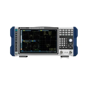
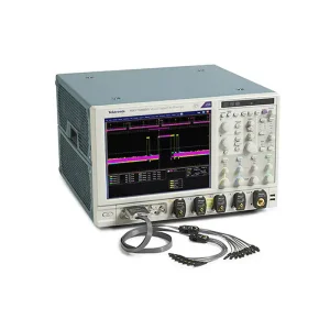
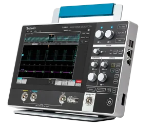
Output ripple and high-frequency switching noise are characterized using a 20 MHz bandwidth limit on a high-speed oscilloscope. Measurements are captured directly at the output pins using a 1:1 probe with a shortened ground spring contact (avoiding ground clip antenna loops), terminated in parallel with a 0.1 µF ceramic capacitor and a 10 µF electrolytic capacitor.
Isolated converters incorporate galvanic isolation via high-frequency transformers, physically separating input and output ground domains. This prevents ground loops, satisfies high-voltage safety isolation, and protects sensitive computing loads from noisy input busses. Non-isolated converters (buck, boost) share a common ground reference, achieving higher conversion efficiency and lower bill-of-materials costs at the expense of galvanic separation.
Gallium Nitride semiconductors feature ultra-low on-resistance ($R_{DS(on)}$) and zero reverse recovery charge, reducing combined conduction and switching losses by up to 50% compared to silicon. This efficiency leap cuts internal heat dissipation drastically, enabling smaller passive heatsinks, reducing airflow requirements, or facilitating completely fanless, potted convection-cooled enclosures.
Industrial units generally require certification under IEC/EN/UL 62368-1 for general electronic/IT gear, or IEC 61010-1 for measurement and control equipment. In Europe, CE marking requires compliance with both the Low Voltage Directive (LVD) and EMC Directive (EN 55032 / EN 55035). North American deployment mandates OSHA Nationally Recognized Testing Laboratory (NRTL) listings, such as UL or CSA marks.
Yes. Professional suppliers provide full lifecycle support including factory recalibration of digital telemetry nodes, voltage trimming, firmware reflashing, and component-level repair. Standard test equipment such as multimeters, oscilloscopes, and automated electrical calibration benches ensure long-term precision throughout the product lifecycle.
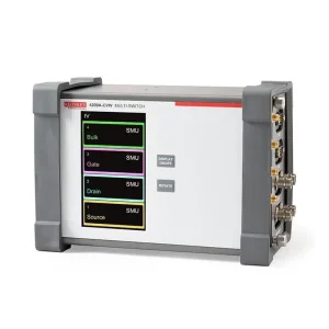
Essential testing hardware for comprehensive electrical calibration, pressure measurement, dynamic current waveform analysis, and semiconductor parameter characterization.