Explore Tier-1 calibrated instrumentation, optically isolated high-common-mode probing, and digital acquisition engines engineered for high-fidelity waveform reconstruction.
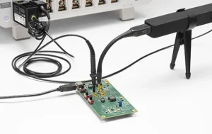
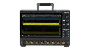
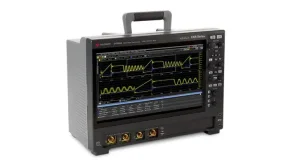
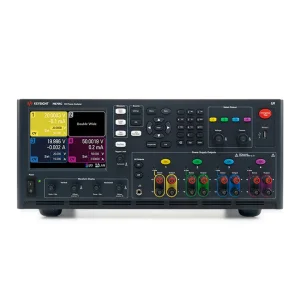
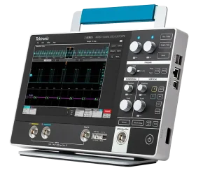
As switching speeds exceed nanosecond thresholds and wide-bandgap semiconductors dominate modern topologies, measurement accuracy depends critically on probe tip interface dynamics.
Traditional differential probes suffer severe common-mode rejection degradation at frequencies over 50 MHz. Advanced electro-optic isolation topologies (such as IsoVu technology) convert raw analog sensor currents into modulated optical signals. This design achieves complete galvanic barrier isolation, virtually eliminating ground loops and maintaining over 80 dB CMRR even at gigahertz ranges when evaluating high-side GaN and SiC floating gates.
Modern high-speed serial protocols (PCIe 5.0/6.0, PAM4 DDR5 memory interfaces) present fragile link budgets. Modern active differential probes integrate high-impedance GaAs and SiGe custom ASICs directly at the replaceable tip head, dropping circuit capacitive loading beneath 0.3 pF to avoid resonant ringing and circuit detuning.
Power integrity demands sub-millivolt ripple analysis superimposed upon multi-volt rails. Dedicated rail probes incorporate exceptionally low DC loading with 50-kΩ input impedances, large built-in offset voltage ranges up to ±60V, and broad bandwidth past 4 GHz, overcoming the frequency roll-off and noise floor degradation of legacy 10:1 passive probes.
Tier-1 manufacturing operations and research labs apply rigorous metrology and lifecycle metrics when procuring precision probes and measurement infrastructure.
System bandwidth must comfortably exceed the fifth harmonic of the target signal. For digital edge transitions, rise-time fidelity dictates that probe rise time should be less than one-third of the signal edge transition (tr_measured = √(tr_signal2 + tr_probe2)).
Power electronics evaluation requires differential ranges extending up to 6 kV with certified CAT ratings, while high-speed digital buses demand sensitivity down to 10 mV/div without injecting internal amplifier thermal noise into phase jitter computations.
Dense board layouts offer virtually zero physical test pad clearance. Enterprise buyers verify the availability of high-density solder-in micro-tips, browser tips with flex capability, high-temperature environmental chamber extension cables, and MMCX/SMP coaxial interface attachments.
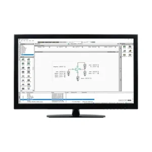
Intelligent digital interfaces communicate probe attenuation, serial data, and temperature coefficients to the scope host. Factory-characterized S-parameters are dynamically de-embedded in real time from raw acquisitions.
From electric vehicle powertrains to multi-lane multi-gigabit backplanes, test configurations must pair specialized probes with optimized front-end hardware.
High-voltage traction inverters operate at fast switching slews (dv/dt > 100 V/ns). Coupling optically isolated differential voltage probes with high-frequency Rogowski coils ensures precise switching energy (Eon, Eoff) captures without dangerous ground bounce or false shoot-through trigger artifacts.
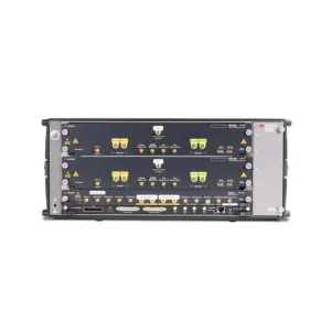
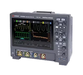
Analyzing high-speed memory and bus traffic requires synchronized acquisition across multiple points. Combining low-capacitive active differential probes with multi-channel digitizers and high-definition oscilloscopes enables multi-lane jitter decomposition and protocol compliance verification without load distortion.
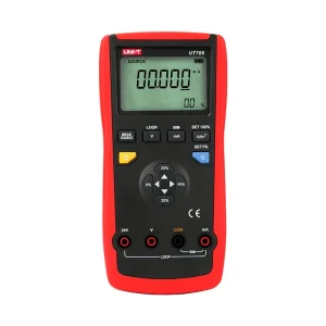
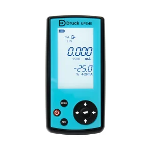
Traceability guarantees measurement confidence across production lines. Deploying certified electrical calibrators and transfer standards validates probe attenuation ratios, input resistance, capacitive balance, and high-frequency rise-time responses across strict environmental envelopes.
Machine-Win establishes rigorous export verification, NIST/ISO calibration workflows, and supply-chain transparency for precision electronic test assets.
Every active probe head, mainframe, and accessory package ships brand-new and factory-original with uninterrupted serial traceability, manufacturer certificates of conformance, and direct warranty verification capabilities.
Calibration regimens adhere to ISO/IEC 17025 accredited standards. Before global dispatch, our metrology engineers confirm DC gain error, AC response flatness, tip capacitive balance, and baseline noise floors.
High-frequency probe heads contain sensitive ceramic substrates and GaAs die structures vulnerable to micro-impacts. Shipments utilize specialized anti-static enclosures, custom foam cradles, and monitored transit documentation across 100+ countries.
A strategic overview of emerging architectural shifts shaping test interfaces through 2028 and beyond.
Widespread adoption of galvanic electro-optic isolation heads for wide-bandgap compound semiconductor switching analysis. Broad deployment of 50-kΩ power rail probes to identify microvolt rail sag on complex AI accelerator package topologies.
Transition toward micro-machined MEMS contactors and direct silicon interposer probe points. Autonomous compensation networks embedded in probe tip assemblies mitigate skin-effect losses and ground-loop parasitic inductance up to 30 GHz.
Integration of coherent optical transceivers inside the probe interface, facilitating near-zero mechanical loading directly onto sub-micron interconnects. Real-time neural network compensation algorithms correct non-linear signal distortions instantaneously.
Essential guidance on selecting, calibrating, and maintaining high-performance oscilloscope probing solutions.
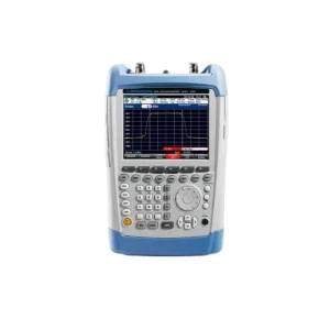
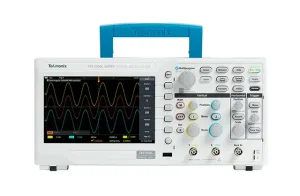
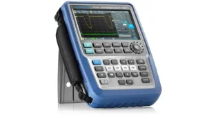
Complete your laboratory bench with traceable reference calibrators, spectrum analyzers, portable digital oscilloscopes, and automated measurement frames.